Psi-k workshop on
“Atomic scale materials microscopy: theory meets experiment”
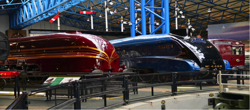
National Railway Museum, York (UK)
26-28 June 2017
Summary:
Atomic scale materials characterization is now one of the major drivers of technological innovation in areas such as nanoelectronics, catalysis, medicine, clean energy generation and energy storage. This can in a large part be attributed to advances in electron and scanning probe microscopies, which are now able to provide atomically resolved structural, chemical and electronic characterization of a wide range of functional materials. However, the types of systems relevant to applications, which include surfaces, interfaces, nanocrystals and two-dimensional materials, are complex and interpreting experimental images and spectra is often extremely challenging. On the other hand, parallel advances in theoretical approaches means that theory can often offer invaluable guidance. These approaches include first principles methods for structure prediction, simulation of scanning probe and electron microscopy images, and prediction of various spectroscopic signatures (e.g. EELS and STS). Some of the most impressive examples of this kind of research in recent years have combined complementary theoretical and experimental approaches in a synergistic way to unravel the complex structure of materials. This type of integrated approach is increasingly being recognised as critical to advanced materials research and development by both industry and research funders.
It was in this context that the Psi-k workshop: “Atomic scale materials microscopy: theory meets experiment” was held between the 26th and 28th of June 2017 at the National Railway Museum in York (UK). The scientific focus was on the application and development of first principles methods that, in synergy with advanced microscopy techniques (e.g. TEM, EELS, STM, AFM), can help to unravel the structure and properties of materials at the atomic scale. Open to both experts and newcomers the aim was to provide a rounded overview of emerging methods and challenges in the field, and provide an opportunity for in-depth discussion and exchange of ideas.
The workshop was organized by Keith McKenna and Phil Hasnip (Department of Physics, University of York, UK) and Adam Foster (Department of Applied Physics, Aalto University, Finland). The workshop received funding from Psi-k (www.psi-k.net) and UKCP (www.ukcp.ac.uk).
Documents:
- Workshop website: https://www.asmm.sciencesconf.org/
- Abstract book
List of participants:
- Jonathan Bean – University of York
- John J Carey – University of York
- Scott Chambers – Pacific Northwest National Laboratory
- János Daru – Ruhr-Universität Bochum
- Joyashish Debgupta – University of York
- Razak Elmaslmane – University of York
- Andrea Floris – University of Lincoln
- Adam Foster – Aalto University
- Thomas Frederiksen – Donostia International Physics Center
- Julian Gaberle – University College London
- Arsham Ghasemi – University of York
- Phil Hasnip – University of York
- Cécile Hébert – École Polytechnique Fédérale de Lausanne
- Steven Hung – University of York
- Demie Kepaptsoglou – SuperSTEM
- Adam Kerrigan – University of York
- Roland Kroger – University of York
- Vlado Lazarov – University of York
- Sabrina Masur – University of Cambridge
- Keith McKenna – University of York
- Tim Naginey – University of Oxford
- Genadi Naydenov – University of York
- Rebecca Nicholls – University of Oxford
- Omar Omar – University of York
- Claudio Padilha – University of York
- Rossitza Pentcheva – University of Duisburg-Essen
- Leon Petit – STFC
- Daniel Pingstone – University of York
- Andrew Pratt – University of York
- Matt Probert – University of York
- Georg Schusteritsch – University of Cambridge
- Martin Setvin – TU Wien
- Ashish Suri – University of York
- Edward Tait – University of Cambridge
- Steve Tear – University of York
- Chris Walker – University of York
- Jamie Warner – University of Oxford (Cancelled)
- Matt Watkins – University of Lincoln
- Viktor Zólyomi – University of Manchester
Programme:
Monday 26th June
13.00 Registration and coffee/tea
Session 1 (chair: Adam Foster)
13.30 Martin Setvin (TU Wien, Austria)
I1. Cleaved KTaO3 surfaces studied by combined AFM/STM
14.20 Matt Watkins (University of Lincoln, United Kingdom)
C1. 3D molecular resolution at solvated Fluorite (111) surface: theory meets experiment
14.45 Julian Gaberle (University College London, United Kingdom)
C2. Combining Theory and Experiment to Study Self Assembly of Organic Molecules on an Insulating Surface
15.10 Coffee/tea break
15.40 Thomas Frederiksen (Donostia International Physics Center, Spain)
I2. First-principles transport methods for nanoelectronics
16.30 János Daru (Lehrstuhl fur Theoretische Chemie, Ruhr-Universität Bochum, Germany)
C3. Solvation in 2D: Microsolvated Ions on Inert Surfaces
17.00 Close of session
Tuesday 27th June
Session 2 (chair: Scott Chambers)
09.00 Cécile Hébert (École Polytechnique Fédérale de Lausanne, Switzerland)
I3. Transmission electron microscopy: new advances and why we need theory
09.50 Daniel Pingstone (University of York, United Kingdom)
C4. Polar MgO(111)/SiC(0001): atomic structure and electronic properties
10.15 Coffee/tea break
10.45 Rossitza Pentcheva (University of Duisburg-Essen, United Kingdom)
I4. Designing electronic phases at oxide interfaces for electronic, spintronic and energy applications
11.35 Georg Schusteritsch (University of Cambridge, United Kingdom)
C5. Predicting the structure of interfaces using the Ab Initio Random Structure Searching method
12.00 Lunch and discussion time
Session 3 (chair: Cecile Hebert)
14.00 Rebecca Nicholls (University of Oxford, United Kingdom)
I5. Enhancing materials design using microscopy and modelling
14.50 Edward Tait (University of Cambridge, United Kingdom)
C6. Simulation of electron energy loss spectra of nanomaterials with linear-scaling density functional theory
15.15 Arsham Ghasemi (University of York, United Kingdom)
C7. Van der Waals interfaces: TI/superconductor and semiconductor
15.40 Coffee/tea break
16.10 Scott Chambers (Pacific Northwest National Laboratory, United States)
I6. Understanding complex phenomena at complex oxides interfaces by STEM/EELS/EDS and theoretical modeling
17.00 Close of session
18.00 Informal workshop dinner (BrewDog York)
Wednesday 28th June
Session 4 (chair: Rebecca Nicholls)
09.00 Vlado Lazarov (University of York, United Kingdom)
I7. Structure – Functionality Correlation of Halfmetalic Materials for Spintronics
09.50 Jonathan Bean (University of York, United Kingdom)
C8. Atomic structure and electronic properties of MgO grain boundaries in tunnelling mag- netoresistive devices
10.15 Andrea Floris (University of Lincoln, United Kingdom)
C9. Mechanisms of Covalent Dimerization on a Bulk Insulating Surface
10.40 Coffee/tea break
11.10 Jamie Warner (University of Oxford, United Kingdom)
I8. The atomic structure and dynamics of defects in 2D materials – WITHDRAWN
12.00 Viktor Zólyomi (University of Manchester, United Kingdom)
C10. Anomalous optical response in atomically thin InSe
12.25 Tim Naginey (University of Oxford, United Kingdom)
C11. Including the effects of atomic bonding in (S)TEM image simulation
12.50 Close of Workshop
Scientific summary:
A generous 50 minutes was allocated for invited talks and 25 minutes for contributed talks with plenty of time for questions, and there was a constructive and interesting discussion following every talk.
The first day focused primarily on scanning probe techniques (STM and AFM). A common theme in all of the talks was importance of combining theory and experiment to help understand the structure of complex surfaces, including for example KTaO3 (Martin Setvin, TU Wien) and solvated fluorite (Matt Watkins, University of Lincoln). We also heard from Thomas Frederiksen (Donostia International Physics Centre) about state-of-the-art theoretical methods for modelling electron transport with relevance for scanning probe microscopies and molecular electronics.
The second and third days focused primarily on transmission electron microscopy (TEM) and associated techniques such as energy loss spectroscopy. The first invited talk of the second day was given by Cécile Hébert (École Polytechnique Fédérale de Lausanne, Switzerland) and gave an excellent introduction to TEM techniques and recent advances. Over the remaining two days we saw many examples of advances in theoretical simulation and experimental techniques which together are helping to resolve the atomic structure of increasingly more complex materials and defects. This included the application of ab initio random structure searching to predict the structure complex grain boundary interfaces in TiO2 (Georg Schusteritsch, University of Cambridge), EELS modelling to identify chemical bonds in N-doped graphene (Rebecca Nicholls, University of Oxford), the development of EELS simulation in linear scaling DFT (Edward Tait, University of Cambridge), the complementary use of STEM, EELS ad EDS to resolve the structure of complex oxide interfaces (Scott Chambers, Pacific Northwest National Laboratory), and many more.
Evaluation:
Following the workshop a short survey was sent to participants. A summary of the feedback is given below.
Quality of the scientific programme (invited and contributed talks):
- Excellent (74%)
- Above average (26%)
- Average (0%)
- Below average (0%)
- Poor (0%)
Would you attend a similar workshop if another were to be held in the future?:
- Yes (87%)
- Maybe (13%)
- No (0%)
Anonymous comments:
‘A very well organised workshop!!’
‘All together a great event’