
Rome, Italy, 18-19 December 2017
Organisers:
-Maurizia Palummo, Physics Department Tor Vergata University, Rome, Italy
-Giacomo Giorgi, Department of Civil & Environmental Engineering (DICA) University of Perugia, Italy
-Jeffrey Grossman, Materials Science Department MIT, Boston, USA
Funding: Psi-K
Introduction
Isolating graphene for the first time in 2004, with its plethora of possible device⎯oriented appealing features, has paved the way towards the study of several new classes of layered two-dimensional (2D) materials. In several opto-electronic applications such as those involving the solar-to energy conversion process, it is indeed extremely appealing to control the properties of well-understood 3D materials by reducing their dimensionality towards the 2D limit or, even better, to directly focus on naturally layered materials both free⎯standing and also coupled with other layered ones in order to boost the sunlight conversion efficiency. Moreover, stacked Van der Waals (vdW) heterostructures of 2D monolayers offer a unique playground to engineer the opto⎯electronic properties towards the realization of devices with different functionalities and with the availability of metallic, semiconducting, and insulating materials. Due to their high surface to volume/ratio 2D⎯layered materials can harvest solar energy and generate electrons and holes, and they can also provide paths for the separation and diffusion of the photo-excited carriers. These are fundamental prerequisites for the realization of any photo⎯catalytic or photovoltaic cell. The use of these emerging two-dimensional layered materials in technological applications presupposes a detailed knowledge of their chemical and physical properties. Theoretical methods and simulations play a fundamental role for the understanding and predicting these properties. The goal of the workshop, collecting distinguished scientists in the field, has been to clarify the theoretical microscopic understanding of layered 2D Materials with a particular focus on applications in opto-electronics and solar⎯to⎯energy conversion. An overview of the research at experimental level from experts in the field has also been given.
Summary
The participants gathered at 10 am of December 18th in front of the Urbano VIII room in the Cecam Italian node Simul located in Via Madonna dei Monti 40, Rome. Maurizia Palummo from Tor Vergata University welcomed everyone and introduced the daily format, poster session and the social event.
The Director of the Node, Prof. Antonio di Carlo, has introduced the mission that the Simul Node towards scientific initiatives like the present one. The Node staff has been extremely efficient and helpful and contributed to make the workshop successful.
Overall, the structure of the workshop has been constituted by three main branch topics: Transition Metal Dichalcogenides (TMDs), 2D Hybrid Organic Inorganic Perovskites (OIHPs), and other layered materials for optoelectronics.
With his seminar focusing on the nature of Quantum Confinement (QC) and its extension to rational design of novel materials, Thomas Heine from Leipzig University, Germany, has opened the event stressing the concept of QC as a driving force not only in Quantum Dots but also in layered materials. In particular, starting from layered materials like chalcogenides where the gap is indirect, “peeling” up to the single layer QC shows its role in making the gap direct and accordingly to make the sheet extremely appealing for optoelectronic applications.
The second talk of the first session has been given by Kristian Thygesen from the Technical University of Denmark. He has introduced the concept of van der Waals heterostructure and how this architecture can be used in the controlling the dielectric function of a layered material. Furthermore he has discussed the properties of a novel material, TaS2, where optical losses are reduced due to the superior properties of the material. These results, as those of Thomas Heine, pave the way towards “intelligent” materials for optoelectronics.
Third one in the morning has been Francesco Mauri (Rome University, “La Sapienza”) who, at variance with the first two seminars, has focused his investigation on the magnetic properties of a more assessed material, i.e. graphene but in the rhomboedral form. In particular, the goal here has been to point out the applicability of graphene to spintronics.
The last Invited Speaker of the first session has been Olivia Pulci from “Tor Vergata” University of Rome. In her seminar, she has provided theoretical support, by means of a combined DFT-GW-BSE approach, to the widely experimentally reported applicability of 2D nitrides in optoelectronics. In particular, GaN and InN are calculated to have a direct gap on gamma point, making them extremely appealing for device oriented applications. Additionally, Olivia Pulci has discussed the possibility of stacking these materials with the result of obtaining novel architectures for PV and solar harvesting applications.
Lunch has been the first chance of getting together and discussing about shown results and perspectives among Participants and Invited Speakers. It is worth mentioning that the venue of the workshop, located in one of the most cozy and beautiful spots of the city, has offered a wide choice of bars and restaurants providing ideal and relaxing places for scientific discussions even during lunch breaks.
Chair of the first afternoon session has been Jeffrey Grossman.
First Invited Speaker of the session has been Miguel Pruneda from the Catalan Institute of Nanotechnology. In his speech he reviewed the concept of polar discontinuities in 2D materials and discussed how this is related to 1D metallic states at mirror twin boundaries in semiconducting MoSe2 monolayers and can explain the formation of a CDW at low temperature.
Then Giancarlo Cicero focused on the possibility to stabilize the T-phase of MoS2 and WS2 using molecular functionalization and doping, showing also the extreme tunability of the electronic and optical properties.
Andrea Marini illustrated how the Non-Equilibrium Green Function approach can now be used in a complete ab-initio framework to study ultra-fast phenomena in 2D materials showing very interesting results for MoS2 and WSe2.
Marco Bernardi reviewed the absorbance and light emission status of the group-VI TMD, showing the potential of these materials for solar-energy conversion. He illustrated how to obtain ab-initio radiative recombination rates in very good agreement with experimental data and lastly focused on how to interpret the anisotropic photoluminescence seen experimentally in TMDs excited with linearly polarized light.
After the coffee-break during which a poster session from mainly young participants to the workshop has been held, Marco Bernardi chaired the last session of the day.
Can Ataca showed how post-transition metal chalcogenides (PTMCs), 2D-GaSe sheets, display vastly different phenomena under strain with a strong increase of the PL intensity under strain. Moreover a colossal optical absorption anisotropy of GaSe has been discussed suggesting that the light–matter interaction and the optical properties of 2D-GaSe can be controlled at will by manipulating the optical absorption. The same speaker introduced the experimental speech on TMD membranes of Seffaattin Tongay who could not join the workshop for last minute problems
The last speech of the day was another experimental one from Antonio Polimeni who discussed the effects of proton-irradiation in TMD which leads to the formation of domes able to emit light at RT. By demonstrating the possibility to change size and position of the domes by lithographic approaches he paved the way to control the opto-electronic properties of TMD on large, scalable regions
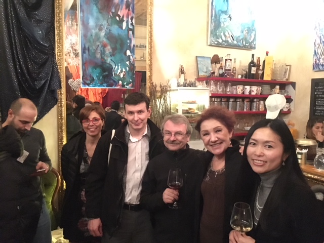
The social event has been organized at the Caffe Bohemien, a small cafeteria where all the Participants and the Speakers had the possibility to enjoy a lively atmosphere with good food and wine
The workshop second day morning first session has started under the supervision of Koichi Yamashita from Tokyo University who has chaired the session opened by the seminar of Aldo Di Carlo.
 i
i
This Seminar mainly experimental, has been chosen in order to open the section of the workshop mainly dedicated to the so called Hybrid Organic-Inorganic Halide Perovskites (OIHPs).
In particular, he illustrated which is the experimental state of the art of OHIPs solar cells, showing how the introduction of 2D materials can improve their PV efficiency and largely increase the tunability of their opto-electronic properties.
After Aldo Di Carlo speech, a more theoretical oriented session has been opened by the seminar of Claudine Katan from Rennes University who has focused on the properties of layered perovskites with particular attention paid to the so called Ruddlesden-Popper perovskites: comparison among DFT and BSE results and low-temperature high-field magneto-absorption experiments have been similarly reported and discussed by Claudine Katan. Maurizio Cossi from University of Eastern Piedmont has shown then his theoretical findings from an analysis of 2D perovskites formed by Pb and Sn, both iodides and bromides, intercalated by mono- and divalent organic cations. He similarly has shown the trend of band gaps for PbI4, PbBr4 ad SnI4 systems with different series of cations, and the correlation of electronic properties with some geometrical parameters.Last Speaker of the first session of the morning has been Edoardo Mosconi from Italian CNR. In his seminar he has provided an overview of the research activity of his group in the OIHPs field with particular focus on the stability of 2D/3D heterostructures.
Giacomo Giorgi chaired the next session of the day introducing Koichi Yamashita from Tokyo University. In his talk he demonstrated that the charge separation is induced by the structural fluctuation of the inorganic lattice using first-principles molecular dynamics simulations and has shown how charge carrier trapping at defects on surfaces or grain boundaries are one of the main limiting factors for carrier lifetime.
In his speech Olexander Voznyy has shown how 2D and quasi-2D lead-halide peroskytes are characterized by strong electron-hole and exciton-exciton interactions which open the way to new opportunities for electrical modulation of absorption edge, Bose-Einstein condensation at room temperatures, and spin polarization without external magnetic fields.
The focus of Daniele Varsano talk has been on anatase 2D-nanosheets and in particular on the role of quantum-confinement on their electronic and optical properties, discussing the differences the between the (001) and (101) surface terminations.
Conor Hogan discussed the structure and optical properties of various silicene-like systems: freestanding silicene, silicon nanoribbons formed on Ag(110), and silicene 2D sheets on Ag(111) as obtained by first-principles calculations.
Olivia Pulci from Tor Vergata University chaired the last session of the workshop. The first speaker, Myrta Gruning, introduced a recently developed real-time approach which allows to calculate non-linear optical properties of materials in a complete ab-initio framework, with the inclusion of Many-body effects within the Green’s function theory.. She illustrated the application of this method to several 2D layered materials (MoS2, h-BN, GaN, ZnO, SiO2).
Pawel Hawrylak from Ottawa University has given a seminar focused on the electronic properties of graphene, WS2 and MoS2 . In particular, results of a tight-binding model approach involving Mo and W metal d-orbitals and sulfur dimer S2 p orbitals, model obtained via ab-initio calculations, are then reported and analogies and differences with graphene quantum dots are introduced in the discussion of exciton spectrum.
Davide Campi from EPFL concluded the workshop showing how high-throughput approaches are able at identifying new promising 2D candidates for electronic, optoelectronic and energy applications.
Programme
December 18th 2017
10.00-10.30 Registration/Coffee break
10.30-10.45 Welcome of Cecam Simul Node Director
10.45-11.00 Introduction
Chair: Maurizia Palummo
11.00-11.30 Thomas Heine “2D materials with strong quantum confinement for optoelectronics and photocatalysis”
11.30-12.00 Kristian Thygesen “2D layered crystals for plasmonics and optical meta-materials”
12.00-12.30 Francesco Mauri “Magnetic Band-Gap Opening Rhombohedral-stacked Graphene: a platform for spintronic devices”
12.30-13.00 Olivia Pulci “Tunable electronic properties of two-dimensional nitrides for light harvesting heterostructures”
13.00-14.00 Lunch
Chair: Jeffrey Grossman
14.00-14.30 Miguel Pruneda “Electronic instabilities and metallic grain boundaries in dichalcogenides”
14.30-15.00 Giancarlo Cicero DISAT“MoS2 enhanced T-phase stabilization and tunability through alloying and organic functionalization”
15.00-15.30 Andrea Marini“Ab initio simulations of ultra-fast dynamics in two-dimensional materials”
15.30-16.00 Marco Bernardi, “Light-Matter Interaction in Two-Dimensional Transition Metal Dichalcogenides“
16.00-17.00 Coffee-break & Posters
Chair: Marco Bernardi
17.00-17:3.00 Can Ataca “Post Transition Metal Chalcogenides for Device Applications”
17:30-18:00 Can Ataca (on behalf of Seffattin Tongay) ” Fundamentals of anisotropic atomically thin membranes”
18.00-18.30 Antonio Polimeni “Proton-driven generation of atomically thin, light emitting domes in transition metal dichalcogenides”
December 19th 2017
Chair: Koichi Yamashita
9.00-9.30 Aldo Di Carlo “2D materials for hybrid organic/inorganic photovoltaics”
9.30-10.00 Claudine Katan “Insight from theory on optoelectronic properties of layered hybrid perovskites”
10.00-10.30 Maurizio Cossi ”Ab initio design of 2D Hybrid Organohalide Perovskites with Tunable Band Gap”
10.30-11.00 Edoardo Mosconi “First Principles Modeling of Mixed 2D/3D Organohalide Perovskites“
11.00-11.30 Coffee break & Posters
Chair: Giacomo Giorgi
11.30-12.00 Koichi Yamashita “Charge Separation and Charge Carrier Trapping of Lead Iodide Perovskites”
12.00-12.30 Olexsander Voznyy“Modulating the excitonic interactions in layered 2D and quasi-2D lead halide perovskites”
12.30-12.45 Daniele Varsano “Role of quantum confinment in anatase nanosheets”
12.45-13.00 Conor Hogan “Optical characterization of free-standing and epitaxial silicene“
13.00-14.00 Lunch
Chair: Olivia Pulci
14.00-14.30 Myrta Gruning “Non linear optical spectra in 2D materials”
14.30-15.00 Pawel Hawrylak “Electronic structure, magnetoexcitons and valley polarized electron gas in 2D crystals”
15.00-15.30 Davide Campi “High-throughput search of novel 2d materials for electronic and optoelectronic applications”
15.30-15.45 Conclusions and farewell
POSTERS
“Electronic and optical properties of Dirac materials: the case of Cd3As2” Adriano Mosca Conte
“Photo-electron and thermionic emission from an illuminated phosphorene surface”, Saibabu Madas
“Properties and challenges of 1-D and 2-D polymerization on surfaces” Gianluca Galeotti
“Non-linear optics in 2D materials from first-principles” Myrta Gruning
“Excitonic effects in 2D Nitrides” Stella Prete
“Electronic and optical properties of graphene-like Si and Ge: Silicene and Germanene” Davide Grassano
“Single walled carbon nanotube/Si and Graphene/Si heterojunctions for high responsivity photodetectors” Mattia Scagliotti
Participants
Stefano Bellucci Laboratori Nazionali Frascati INFN, Italy
Maria Grazia Betti Dipartimento di Fisica Università di Roma “La Sapienza”
Carlo Maria Bertoni, Dipartimento di Fisica Università di Modena e Reggio Emilia, Italy
Elena Blundo Dipartimento di Fisica di Roma ” La Sapienza”
Elena Cannuccia Dipartimento di Fisica Università di Roma “Tor Vergata”
Paola Castrucci Dipartimento di Fisica Università di Roma “Tor Vergata”
Giorgio Contini ISM-CNR Rome, Italy
Riccardo Di Gennaro EPFL Lausanne, Switzerland
Gianluca Galeotti INRS-EMT, Varenne Canada
Paola Gori Dipartimento di Ingegneria Università degli Studi di Roma III
Davide Grassano Dipartimento di Fisica Università di Roma “Tor Vergata”
Myrta Gruning Queen’s University Belfast, U.K.
Leonidas Mouchliadis Institute of Electronic Structure and Laser , FORTH, Heraklion, Crete, Greece.
Saibabu Madas ELI-HU Computational and Applied Materials Science Group Attosecond and Strong Field Science division, Szeged, Hungary
Adriano Mosca Conte MIFP Italy
Alessandro Pecchia ISMN CNR Rome, Italy
Stella Prete Dipartimento di Fisica Università di Roma “Tor Vergata”
Andrea Pianetti Dipartimento di Fisica Università di Roma “Tor Vergata”
Mattia Scagliotti Dipartimento di Fisica Università di Roma “Tor Vergata”
Manuela Scarselli Dipartimento di Fisica Università di Roma “Tor Vergata”
Mikhail Shuba Institute for Nuclear Problem Belarus State University Minsk, Belarus
Davide Tedeschi, Dipartimento di Fisica Università di Roma “La Sapienza”
ABSTRACTS
Enhancing Light Emission Efficiency without Color Change in Post-Transition Metal Chalcogenides
Can Ataca
Department of Physics University of Maryland Baltimore County, USA
Two-dimensional (2D) materials can take a large amount of mechanical deformation before reaching the fracture limit due to their high Young’s modulus, and this in return, provides a way to tune the properties of 2D materials by strain engineering. Previous works have shown that the optical band gap of transition metal chalcogenides (TMDs) can be modulated by strain, resulting in a drift of the
photoluminescence (PL) peak position and a decrease (or little change) in PL intensity. Here, we report a member of the post-transition metal chalcogenides (PTMCs), 2D-GaSe sheets, displaying vastly different phenomena under strain. Strained 2D-GaSe emits photons at almost the same wavelength as unstrained material but appears an order of magnitude brighter. In contrast to TMDs, optical spectroscopy measurements reveal that changes in the optical properties are mostly related to the colossal optical absorption anisotropy of GaSe, instead of commonly accepted strain-induced band renormalization. Results suggest that the light–matter interaction and the optical properties of 2D-GaSe can be controlled at will by manipulating the optical absorption.
Light-Matter Interaction in Two-Dimensional Transition Metal Dichalcogenides
Marco Bernardi
Department of Applied Science Caltech Pasadena USA
Transition metal dichalcogenides (TMDs) exhibit unusual electronic and optical properties. The talk will discuss first-principles calculations of light absorption and emission in TMDs. Using the GW-Bethe Salpeter equation method, we show that absorption per unit thickness in monolayer and few-layer TMDs is 1-2 orders of magnitudes greater than in conventional semiconductors such as silicon and GaAs. Our predicted applications to solar energy conversion, as well as their recent experimental realization, are discussed. We introduce a formalism to compute the radiative recombination rate in TMDs. Our calculations of the radiative lifetimes as a function of temperature are in excellent agreement with experiment, and our results guide the interpretation of ultrafast spectroscopies in monolayer and hetero-bilayer TMDs. Lastly, we focus on the anisotropic photoluminescence seen experimentally upon exciting TMDs with linearly polarized light. We generalize our radiative rate calculations to obtain an equation for light emission rate as a function of angle. Mixing the two lowest bright excitons in their degenerate subspace is shown to lead to excitons in a physically meaningful quantum superposition in the K and K’ valleys, which are responsible for the anisotropic photoluminescence. Non-radiative processes and trions are outlined in closing.”
High-throughput search of novel 2d materials for electronic and optoelectronic applications
Davide Campi
EPFL Lausanne
2D materials provide a novel paradigm and toolbox for materials scientists to discover or engineer new properties and functionalities. However, the handful of 2D materials intensively studied up to now represent only a few of the manifold possibilities. In this work we present the results of a characterization effort and applications-oriented screening that, using state-of-the-art first-principles simulations and automatized high-throughput calculations through the AiiDA platform[1], aims at identifying new promising candidates for electronic, optoelectronic and energy applications, among the hundreds of 2D materials (1844)[2] discovered by performing a ”computational exfoliation” of a dataset of more than 100000 bulk parent structures.
[1] G.Pizzi, A.Cepellotti, R.Sabatini, N.Marzari and B.Kozinsky, Comp. Mat. Sci. 111, 218 (2016).
[2] N.Mounet, M.Gibertini, P.Schwaller, D.Campi, A.Merkys, A.Marrazzo, T.Sohier, I.E.Castelli, A.Cepellotti, G.Pizzi and N.Marzari, in press (2018).
Ab initio design of 2D Hybrid Organohalide Perovskites with Tunable Band Gap
Maurizio Cossi, Alberto Fraccarollo, Leonardo Marchese
Dipartimento di Scienze e Innovazione Tecnologica, Università del Piemonte Orientale, Alessandria, [email protected]
Hybrid organic-inorganic perovskites (HOP) formed by various metal halides and organic cations raised an enormous interest for their excellent performance in sensitized photovoltaic cells (up to 22% energy conversion to date). The best results are obtained with 3D or mixed 3D/2D perovskites (the latter being composed by thick sheets of several 3D layers). Purely 2D HOP (based on lead and tin halogenides) have been studied for opto-electronic applications, but their band gaps are generally too high to allow a direct use in photovoltaics. We have performed a systematic theoretical analysis of 2D perovskites formed by Pb and Sn iodides and bromides, intercalated by mono- and divalent organic cations. The crystal structures are optimized at the DFT level with a program based on localized gaussian-type functions (CRYSTAL17), while the electronic properties were computed with plane wave functions (by QUANTUM ESPRESSO); the band gap calculation includes both spin-orbit coupling (SOC) and post-DFT correlation at the GW level, through the following additive scheme: The results are very interesting: we describe the trend of band gaps for PbI 4, PbBr4 ad SnI4 systems with different series of cations, finding the correlation of electronic properties with geometrical parameters (e.g. interlayer distances). The most intriguing results show that some bications in SnI4 perovskites exhibit small band gaps, compatible with visible absorption, a feature which has not been reported before and opens the way to very interesting developments. We found that the small gaps are associated to empty levels localized in the organic layer, related to low-energy LUMO orbitals in the intercalated cations. Work is in progress to describe the resulting electronic properties (absorption spectra, charge transport), and to assist the experimental synthesis of these compounds.
- Fraccarollo, V. Cantatore, G. Boschetto, L. Marchese, and M. Cossi J. Chem. Phys., 144(16):164701, 2016. A. Fraccarollo, L. Canti, L. Marchese, and M. Cossi J. Chem. Phys., 146(23):234703, 2017. A. Fraccarollo, L. Marchese, and M. Cossi J. Phys. Chem, in press.
MoS2 enhanced T-phase stabilization and tunability through alloying and organic functionalization
Giancarlo Cicero
Dipartimento Scienza Applicata e Tecnologia, Politecnico of Torino, Torino, Italy.
Recently two-dimensional layered materials based on transition metal dichalcogenides (TMD) have received a large amount of attention because of their peculiar and versatile physical properties [1]. Mono and few-layered TMDs are direct-gap semiconductors whose band gap energy, as well as carrier type (n- or p-) varies depending on the composition, structure and dimensionality of the system. In particular, monolayer MoS2 is known to exist in three polymorphs: 2H, 1T and 1T’. The former is thermodynamically stable and semiconducting (Egap=1.68 eV). The metallic 1T structure, on the contrary, was found to be metastable and undergo to a Peierls transition to the 1T’ structure [2]. In the process a small energy gap (0.06 eV) is opened. In recent years, much effort has been made to stabilize T phases over 2H with the aim of gaining enhanced electrical performance, such as lower contact Schottky barriers, or better catalytic activity due to easier electron transfer. Although several techniques were proposed so far, such as alkali metals intercalation and straining, a proper control of the transition is yet to be achieved.
In this theoretical work, we propose two different routes for MoS2 T phases stabilization: alloying with an MX2 material for which the T phase is the thermodynamically stable one or functionalizing the monolayer with organic molecules. As for alloying realization, SnS2 is found to be the best candidate being known to privilege 1T structure over 2H (DE=0.87 eV). Indeed, results carried out by means of Density Functional Theory (DFT) and Cluster Expansion simulations show that, even for small amounts of Sn in MoS2, the T and T’ phases formation energy is reduced making the switch between H and T easier. For low doping concentration, it is also reported that the MoS2 and SnS2 turn into metallic phases, opening up to the creation of metal-semiconductor junctions for PV cells [3]. DFT simulations were also employed to predict MoS2 functionalization with different organic molecules, namely methyl groups and simple aromatic compounds. The proposed molecules are found to chemically bind to the T’ phase of MoS2 monolayer and not to the H one. Our results not only show that these molecules can strongly modify the electronic properties of the MoS2 monolayer and effectively tune its absorption spectra, but also highlight that the stability of the two phases is inverted.
[1] M. Chhowalla et al Nature Chemistry 5, 263 (2013)
[2] M. Calandra et al Phys. Rev. B 88, 245428 (2013)
[3] F. Raffone et al J. Phys. Chem. Lett. 7, 2304 (2016)
2D materials for hybrid organic/inorganic photovoltaics
Aldo Di Carlo
CHOSE – Centre for Hybrid and Organic Solar Energy, University of Rome “Tor Vergata”,
via del Politecnico 1, 00133 Roma, Italy
In the broad context of new generation photovoltaic, perovskite technology gained the interest of the scientific community thanks to the surprising power conversion efficiency (PCE) approaching that of already commercialized thin film photovoltaic, the affordable solution process realization procedures and the possibility to easily scale-up the device’s dimensions from lab-scale to the module. As the matter of the fact, several PSC structures have been proposed in literature with the aim to separately improve the PCE or to extend the device’s lifetime or to reduce the hysteric behavior affecting the device’s current-voltage (I-V) characteristic. In this context, interfaces engineering (IE) approach have been demonstrated to be a winning strategy to finely control the active layer realization and the final device’s performance. Among possible IE alternatives, 2D materials represent a new extraordinary strategy to tune interface properties without modifying absorbing and transporting layers of the PSC. In this communication, we demonstrate the use of graphene and 2D materials as an effective way to both control the morphology and to stabilize the device’s interfaces between perovskite and the charge transporting layers in a mesoscopic PSC structure. The Graphene Interface Engineering (GIE), has several advantages: the 2D nature of the materials matches the dimensionality of interface, ii) there is a large library of 2D materials and iii) 2D materials properties can be easily tuned by proper functionalization. Several strategies have been used to master interface properties by using GIE [1-6] both at the anode and cathode parts of the cell. By dispersing Graphene flakes, produced by liquid phase exfoliation of pristine graphite,[7] into the mesoporous TiO2 layer and by inserting graphene oxide (GO) as interlayer between perovskite and Spiro-OMeTAD layers, we demonstrate a PCE of 18.2% with the two-step deposition procedure, carried out in air.[2] The proposed interface engineering strategy based on GRM has been exploited for the fabrication of state-of-the-art large area perovskite modules. We indeed demonstrated a PCE of 12.6% on a monolithic module with an active area exceeding 50 cm2. The use of 2D materials permitted to increase the PCE by more than 10% with respect to “conventional” modules, i.e. without GIE.[6]. Additional results will be shown for other 2D materials such as MoS2, Lithium neutralized GO, rGO etc.
Acknowledgements
This work has received funding from the European Union’s Horizon 2020 research and innovation programme under grant agreement No. 696656 − GrapheneCore1.
References
[1] A. Agresti et al., Advanced Functional Materials 2016, 26, 2686.
[2] A. Agresti et al. ChemSusChem 2016, 9, 2609
[3] A. Capasso et al. Adv. Energy Mat. 2016, 6, 1600920
[4] T. Gatti et al. Adv. Funct. Mat. 2016, 26, 7443-7453
[5] A. L. Palma et al. Nano Energy 2016, 22, 349
[6] A. Agresti et al. ACS Energy Lett. 2017, 2, 279−287
[7] F. Bonaccorso, et al, Science, 2015, 347, 1246501.
Excitonic effects in nonlinear optical properties of 2D materials
Myrta Grüning1 and Claudio Attaccalite2
1 Queen’s University Belfast – Northern Ireland
2 CiNAM Marseille, CNRS – France
Nonlinear optical properties of 2D materials have been the object of several experimental studies in recent years. In fact, second- and third-harmonic generation can probe noninvasively structural properties (number of layers, layer orientation, symmetry, edges) of layered 2D materials [1]. Furthermore a number of works have suggested that those materials, in particular transition metal dichalcogenides, have a strong nonlinear optical response (e.g second- and third-harmonic generation, intensity-dependent refractive index) with potential applications to e.g. nanophotonic devices [2].
We present a first principles calculation study of nonlinear optical properties of 2D materials. We employ a real-time approach [3] which describes Many-body effects from Green’s function theory [4]. This approach allows us to investigate the role of excitonic effects which are neglected in state-of-the-art simulations, but are deemed extremely important in several experimental works [5]. Assessing the role of excitonic effects is particularly relevant considering it is nontrivial to obtain an absolute measurement of nonlinear optical properties, such as second- and third-harmonic generation. Then it is important to have reliable computational approaches to validate the assumptions made to extract nonlinear optical properties from measurements.
For the second-harmonic generation of several 2D layered materials (MoS2, h-BN, GaN, ZnO, SiO2) we found that at resonance–when compared with independent particle calculations–excitonic effects account for half or more of the spectral intensity [6]. Here we extend the study to the third-harmonic generation–for which in a computational study on 1D nanostructures [7] we found a reduction by one order of magnitude of the spectral intensity when including many-body effects–and the intensity-dependent refractive index in MoS2. Results are compared with recent experimental measurements [8].
[1] See for example Kumar et al (2013), Phys. Rev. B 87, 161403; Yin, X., (2014), Science 344(6183), 488–90.
[2] See for example C. Janisch et al (2014) SciRep 4, 5530; (2014) ACS Nano 8, 2951
[3] Attaccalite, C. & Grüning, M. (2013) Phys Rev B 88, 23, , 235113. , 235113
[4] G. Onida et al Rev. Mod. Phys. 74, 601
[5] G. Wang et al. Phys. Rev. Lett. 114, 097403
[6] M. Grüning, C. Attaccalite Phys. Rev. B 89, 081102 ; C. Attaccalite, A. Nguer, A., E. Cannuccia, and M. Grüning (2015) Phys. Chem. Chem. Phys. 17, 9533-9540
[7] C. Attaccalite, E. Cannuccia and M Grüning (2017) Phys. Rev. B 95, 125403.
[8] A. Säynätjoki et al. ArXiv arXiv:1608.04101v1; G. Wang et al (2015) Photon. Res. 3, A51; Y. Wu et al (2015) PNAS 112, 11800–11805
Electronic structure, magnetoexcitons, and valley polarized electron gas in 2D crystals
Pawel Hawrylak
Department of Physics, University of Ottawa, Ottawa, K1N6N5, Canada
e-mail: [email protected]
We discuss the electronic and optical properties of monolayer 2D hexagonal crystals, graphene and transition metal dichalcogenites (TMDCs), MoS2 and WS2. The ab-initio calculations [1-3] establish TMDCs as direct gap, single monolayer, semiconductors with valley selective optical transitions. In order to develop a better understanding of the electronic properties and their response to external magnetic field a tight binding model involving Mo and W metal d-orbitals and sulfur dimer S2 p orbitals is developed based on input from ab-initio calculations. The role of d- and p-orbitals and nearest and next nearest neighbor hopping is clarified. The effective tight binding model is further reduced to the massive Dirac Fermion model which allows introduction of the magnetic field. The Lande and Zeeman Valley effects and the effect of e-e interactions in the magneto-exciton spectrum are discussed [4]. In the discussion of the exciton spectrum we draw analogies with graphene quantum dots with degenerate top of the valence and bottom of conduction band for which multi-exciton spectrum based on extensive exact diagonalization is known [5]. Finally, we discuss the possibility of broken symmetry ground states of the electron gas, in particular the existence of a Valley Polarized Electron Gas (VPEG), as a ground state of n-type WS2. The Valley Polarized state leads to spontaneous circular polarization of the emitted light, an effect which has been recently observed [3].
*Work in collaboration with M. Bieniek, M. Korkusinski, L. Szulakowska, I.Ozfidan, P. Potasz, A. Petrou and G. Kioseoglou.
[1] Eugene S. Kadantsev and Pawel Hawrylak, Solid State Comm.152, 909 (2012).
[2] M. Bieniek, L. Szulakowska, I.Ozfidan, M. Korkusinski and P.Hawrylak, to be published (2017).
[3] T. Scrace, Y. Tsai, B. Barman, L. Schweidenback, A. Petrou, G. Kioseoglou, I. Ozfidan, M. Korkusinski, and P. Hawrylak, Nature Nanotechnology 10, 603 (2015) .
[4] L. Szulakowska, P.Potasz, M. Bieniek and P. Hawrylak,to be published (2017).
[5] Devrim Guclu, Pawel Potasz, Marek Korkusinski and Pawel Hawrylak,”Graphene Quantum Dots”, Springer-Verlag (2014). P Hawrylak, F Peeters, K Ensslin, Editors, “Carbononics–integrating electronics, photonics and spintronics with graphene quantum dots”, Focus issue, Physica status solidi (RRL)-Rapid Research Letters 10 (1), 11(2016).
2D materials with strong quantum confinement for optoelectronics and photocatalysis
Thomas Heine
Wilhelm-Ostwald-Institut of Physical and Theoretical Chemistry, Leipzig University, Germany
Quantum confinement is one of the design principles in nanotechnology. Well-known examples are quantum dots, which are nanocrystals whose electronic band gaps depend crucially on their spatial extension. Thus, it is possible to create light emitting devices with the colour defined by the diameter of the quantum dot. Latest applications include large-scale displays and lasers.
In my presentation I will show that quantum confinement is not restricted to quantum dots and optoelectronic applications. I will show how quantum confinement can be exploited as strategy for the rational design of functional nanomaterials.
The first examples are taken from the field of layered materials, where quantum confinement can be used to tailor the band gap, but also the character of the band gap. For example, transition metal dichalcogenides MX2 (M=Mo, W, X=S, Se) are indirect band gap semiconductors as bulk and multilayer phases, but direct band gap semiconductors with appreciable photoluminescence signal as single-layer material. These ultrathin materials are also called two-dimensional crystals. The exploitation of quantum confinement gets even more interesting if the symmetry of the material is changed by changing the layer number. For example, by the absence (monolayer) or presence (bilayer) of inversion symmetry in two-dimensional crystals strong spin polarization effects are observed. The strongest quantum confinement effect so far we have predicted for PdS2, a two dimensional crystal that is semiconducting as monolayer, but metallic as bilayer. Similarly, GeP3 is a semiconductor in mono- and bilayer form, but metallic for trilayers and thicker stacks.
Another way of exploiting quantum confinement is the application of external fields, most notably electric fields, which are conveniently applied using a gate voltage, and strain fields. I will present various examples where the electronic band gap and/or the density of states are strongly affected by an external gate voltage and by strain fields. For the latter, I will also show some topological phase transitions.
Finally, I will discuss how 3D materials can be assembled from 2D materials in a way that the intrinsic 2D properties are maintained.
Electronic structure, magnetoexcitons and
valley polarized electron gas in 2D crystals
Pawel Hawrylak*
Department of Physics, University of Ottawa, Ottawa, K1N6N5, Canada
e-mail: [email protected]
We discuss the electronic and optical properties of monolayer 2D hexagonal crystals, graphene and transition metal dichalcogenites (TMDCs), MoS2 and WS2. The ab-initio calculations [1-3] establish TMDCs as direct gap, single monolayer, semiconductors with valley selective optical transitions. In order to develop a better understanding of the electronic properties and their response to external magnetic field a tight binding model involving Mo and W metal d-orbitals and sulfur dimer S2 p orbitals is developed based on input from ab-initio calculations. The role of d- and p-orbitals and nearest and next nearest neighbor hopping is clarified. The effective tight binding model is further reduced to the massive Dirac Fermion model which allows introduction of the magnetic field. The Lande and Zeeman Valley effects and the effect of e-e interactions in the magneto-exciton spectrum are discussed [4]. In the discussion of the exciton spectrum we draw analogies with graphene quantum dots with degenerate top of the valence and bottom of conduction band for which multi-exciton spectrum based on extensive exact diagonalization is known [5]. Finally, we discuss the possibility of broken symmetry ground states of the electron gas, in particular the existence of a Valley Polarized Electron Gas (VPEG), as a ground state of n-type WS2. The Valley Polarized state leads to spontaneous circular polarization of the emitted light, an effect which has been recently observed [3].
*Work in collaboration with M. Bieniek, M. Korkusinski, L. Szulakowska, I.Ozfidan, P. Potasz, A. Petrou and G. Kioseoglou.
[1] Eugene S. Kadantsev and Pawel Hawrylak, Solid State Comm.152, 909 (2012).
[2] M. Bieniek, L. Szulakowska, I.Ozfidan, M. Korkusinski and P.Hawrylak, to be published (2017).
[3] T. Scrace, Y. Tsai, B. Barman, L. Schweidenback, A. Petrou, G. Kioseoglou, I. Ozfidan, M. Korkusinski, and P. Hawrylak, Nature Nanotechnology 10, 603 (2015) .
[4] L. Szulakowska, P.Potasz, M. Bieniek and P. Hawrylak,to be published (2017).
[5] Devrim Guclu, Pawel Potasz, Marek Korkusinski and Pawel Hawrylak,”Graphene Quantum Dots”, Springer-Verlag (2014). P Hawrylak, F Peeters, K Ensslin, Editors, “Carbononics–integrating electronics, photonics and spintronics with graphene quantum dots”, Focus issue, Physica status solidi (RRL)-Rapid Research Letters 10 (1), 11(2016).
Optical characterization of free-standing and epitaxial silicene
- Hogan,1,2 O. Pulci,2,3 P. Gori,4 F. Bechstedt,5 D. S. Martin,6 A. Curcella,7 G. Prevot7, and Y. Borensztein7
1Istituto di Struttura della Materia-CNR (ISM-CNR), Via Fosso del Cavaliere 100, 00133 Rome, Italy
2Dipartimento di Fisica, Universita di Roma “Tor Vergata”, Via della Ricerca Scientifica 1, 00133 Rome, Italy
3INFN, Sezione di Roma Tor Vergata, Via della Ricerca Scientifica 1, 00133 Rome, Italy
4Dipartimento di Ingegneria, Università di Roma Tre, Via della Vasca Navale 79, 00146 Rome, Italy
5IFTO, Friedrich Schiller Universitaet, Max-Wien Platz 1, 07743 Jena, Germany
6Department of Physics, University of Liverpool L69 7ZE, UK
7Sorbonne Université, CNRS-UMR 7588, Institut des NanoSciences de Paris, F-75005, Paris, France
The prediction of silicene [1], a 2D honeycomb crystal of silicon analogous to graphene, lead to intensive theoretical study [2]. Experimental realization has, on the one hand, been successful: although synthesis of free-standing silicene has remained elusive, various reports of silicene growth on Ag(110), Ag(111), ZrB2, and Ir(111) have appeared, culminating in the recent demonstration of a field-effect silicene-based transistor [3]. On the other hand, many of these reports have since been questioned as the strongly hybridized nature of the Si-substrate bonding apparently destroys the key electronic property (Dirac cone) [4].
In this talk we report first principles calculations of the structure and optical properties of various silicene-like systems: freestanding silicene, silicon nanoribbons formed on Ag(110), and silicene 2D sheets on Ag(111). In the case of Si/Ag(110), several structural models have been proposed that suggest a Si-stabilized missing row reconstruction based on zigzag [5] or pentamer [6] chains. Surface optical spectra (reflectance anisotropy spectroscopy RAS and surface differential reflectance spectroscopy SDRS), are interpreted using density-functional theory (DFT) and confirm the correct structure as being a pentamer chain reconstruction [7], definitively ruling out silicene nanoribbon structures [8]. The case of Si/Ag(111) is complicated by the abundance of single and multilayer phases [9], and we attempt to cast light on the atomic geometry by interpreting recent experimental SDRS measurements [9,10] using ab initio DFT simulations of the full Si/Ag overlayer phase. The importance of including many-body effects in the optical spectra calculations of freestanding silicene is examined [11].
[1] G.G Guzman-Verri and L.C. Lew Van Yoon, Phys. Rev. B. 76, 075131 (2007)
[2] See e.g. C. Grazianetti, E. Cinquanta and A. Molle, 2D Mater. 3, 012001 (2016)
[3] L. Tao et al, Nature Nanotechnology 10 227 (2015)
[4] R. Quhe et al, Sci. Rep. 4, 5476 (2014)
[5] C. Hogan et al Phys. Rev. B 92, 115439 (2015).
[6] J. I. Cerdá, et al, Nat. Commun. 7, 13076 (2016).
[7] G. Prévot, C. Hogan, et al, Phys. Rev. Lett. 117, 276102 (2016);
[8] P. De Padova, et al, APL 96, 261905 (2010); B. Aufray et al, APL 96, 183102 (2010); C. Lian and J. Ni, Physica B: Condensed Matter 407, 4695 (2012).
[9] Y. Borensztein et al, Phys. Rev. B. 92, 155407 (2015)
[10] Y. Borensztein, G. Prevot, L. Masson, Physical Review B 89, 245410 (2014);
[11] C. Hogan, O. Pulci, P. Gori, F. Bechstedt, D. S. Martin, A. Curcella, G. Prevot and Y. Borensztein, to be submitted.
Insight from theory on optoelectronic properties of layered hybrid perovskites
Claudine Katan
Institut des sciences chimiques de Rennes, CNRS, Université de Rennes 1, ENSCR, INSA Rennes, FRANCE
- Katan* , B. Traoré, M. Kepenekian, Univ Rennes, Université de Rennes 1, INSA, ENSCR, CNRS, ISCR (Institut des Sciences Chimiques de Rennes) – UMR 6226, Rennes, France W. Nie, J.-C. Blancon, H. Tsai, A. Neukirch, S. Tretiak, A. Mohite, Los Alamos National Laboratory, Los Alamos, New Mexico, USA L. Mao, C. Myae Myae Soe, C. Stoumpos, M. Kanatzidis, Department of Chemistry, Northwestern University, Evanston, Illinois USA L. Pedesseau, J. Even, FOTON, INSA Rennes, Université de Rennes 1, CNRS – UMR 6082, Rennes, France
Solution-processed organometallic halide perovskite have recently emerged as promising absorbers in the realm of photovoltaic technology. During the first years of this “perovskite boom”, attention has been drawn on 3D structural networks with methylammonium lead iodide as the superstar. More recently, layered hybrid perovskites gained renewed interest for several reasons, among which increased stability and room for chemical design as well as broader perspectives for technological advances. In the last few months, several families of phase-pure n-layered perovskites (n number of octahedron in the perovskite layer sandwiched between two organic layers) have been synthetized and shown to demonstrate key features promising for both fundamental physics and improved devices.1 Here, starting from our early theoretical contribution on a 1-layered lead-halide perovskite, 2 which has highlighted differences with conventional semiconductors and importance of relativistic effects, we will investigate through a couple of examples quantum3-6 and dielectric4-8 confinement, excitons in bulk5,8,9 and their fate on the surface10,11 as well as the composite nature of this class of semiconductors that facilitates the determination of band alignments3,6 and offers a framework suited to provide design principles6,9,11 for next generation technologies. The theoretical modeling capitalizes on available DFT codes, development of DFT-based methodologies including empirical resolution of the Bethe-Salpeter Equation that leads to quantitative agreement with exciton binding energies as determined by low-temperature high-field magneto-absorption experiments.9
References
1 H. Tsai et al, Nature 2016, 536, 312; L. Mao et al, JACS 2017, 39, 11956; C. Myae Myae Soe et al, JACS 2017, 139, 16297;
2 J. Even et al, Phys. Rev. B 2012, 86, 205301 (2012); J. Phys. Chem. Lett. 2013, 4, 2999 ;
3 J. Even et al, ChemPhysChem 2014, 15, 3733; J. Phys. Chem. C 2015, 119, 10161 ;
4 D. Sapori et al, Nanoscale 2016, 8, 6369;
5 L. Pedesseau et al, ACS Nano 2016 016, 10, 9776;
6 B. Traore et al. Submitted;
7 J. Even et al. PCCP, 2014, 16, 25182;
8 M. Smith et al, Chem. Sci. 2017;
9 J. C. Blancon et al, arXiv:1710.07653
10 J. C. Blancon et al, Science 2017, 355, 1288;
11 M. Kepenekian et al. To be submitted
Magnetic Band-Gap Opening Rhombohedral-stacked Graphene: a platform for spintronic devices
Francesco Mauri
Dipartimento di Fisica Università di Roma “ La Sapienza”
The realization of modern spintronic devices requires injection of spin-polarized currents. Materials of choice for such devices are half-metals, namely compounds conducting in one spin channel and insulating in the other. Half-metallicity embedded in surface or edge states of an easily processable material like carbon would be an ideal solution. However, carbon is not magnetic in its bulk forms. Recently, it has been shown that multilayer graphene with rhombohedral stacking displays a robust antiferromagnetic surface state. Here, by using first-principles calculations, we show that field-effect doping of these graphene multilayers induces a perfect half-metallic behaviour with 100% of spin current polarization already at dopings attainable in conventional field effect transistors with solid state dielectrics. Our work defines a new kind of spintronic devices where the transition between the low resistance and the high resistance state is driven only by electric field
First Principles Modeling of Mixed 2D/3D Organohalide Perovskites
Edoardo Mosconi
Computational Laboratory for Hybrid/Organic Photovoltaics (CLHYO), CNR-ISTM, Via Elce di Sotto 8, I-06123, Perugia, Italy
Organohalide perovskites hold the promise to be the near-future solution to harness solar energy. Despite the impressive photovoltaic performances of perovskite solar cells, most reported devices are not stable under operation, failing by far the market requirements demanding 25-years lifetime. Diverse technological approaches have been proposed to overcome the instability problem, which, while delivering appreciable improvements, are still far from a market-proof solution. Here we demonstrate one-year stable perovskite solar cells by engineering an ultra-stable 2D/3D HOOC(CH2)2NH3)2PbI4/CH3NH3PbI3 perovskite junction. The 2D/3D composite delivers an exceptional gradually organized multidimensional structure that yields up to 12.9% photovoltaic efficiency in a hole-conductor free architecture. As seen in Fig. 1, there is a 0.14 eV CB upshift at the 2D/2D interface compared to the bulk of the 3D perovskite, which induces a 0.09 eV larger interface gap compared to the 3D bulk. This is clearly consistent with the PL blue shift experimentally observed (0.13 eV) when probing from the mesoporous oxide side. These results suggest that the 2D/3D interaction widens the 3D perovskite band gap in the interface region. Additionally, the thin 2D layer does not constitute a barrier to electron injection to TiO2, but it rather constitutes a barrier towards electron recombination, since the 2D conduction band is found at lower energy than that of the 3D CB. To demonstrate the up-scale potential of this technology we fabricate 10×10 cm2 solar modules by a fully printable, industrial-scale process delivering 11.2% efficient devices which are stable for >9,000 hours with zero-loss in efficiency. These innovative architecture will likely enable the timely commercialization of perovskite solar cells.
Fig. 1. Local Density of state (DOS) of the 3D/2D interface and (B) interface structure with the 2D phase contacting the TiO2 surfaceC Partial DOS summed on the 2D and 3D fragments calculated by SOC (inset) and without. Notice favorable alignment of conduction band states for electron injection into TiO2.
References:
Grancini, G.; Roldán-Carmona, C.; Zimmermann, I.; Mosconi, E.; Lee, X.; Martineau, D.; Narbey, S.; Oswald, F.; De Angelis, F.; Graetzel, M., et al. One-Year stable perovskite solar cells by 2D/3D interface engineering. Nat Commun 2017, 8, 15684.
Two-dimensional Nitrides for Ultraviolet to Infrared detectors
M.S. Prete(1), P. Gori(2) , A. Mosca Conte(3) , F. Bechstedt(4), O. Pulci(1,3)
(1) Dipartimento di Fisica, and INFN, Universita’ di Roma Tor Vergata, Italy
(2) Dipartimento di Ingegneria, Universita’ di Roma 3, Italy
(3) European Theoretical Spectroscopy Facility (ETSF), and Mediterranean Institute for Fundamental Physics
(4) Friedrich Schiller Universität, Jena, Germany
Group-III Nitrides have received great attention for high-power electronic devices and for optoelectronic applications such as light-emitting diodes. In particular, in 2014 Akasaki, Amano e Nakamura were awarded for bright and highly efficient blue LEDs with the Nobel Prize in Physics [1]. In addition, in recent years, theoretical and experimental studies on graphene have provided a wide range of knowledge for a new class of 2D materials [2-3-4-5-6]. Motivated by these recent developments, we present here a systematic ab-initio study of the electronic and optical properties of two-dimensional Nitrides (BN, AlN, GaN, InN, TlN). In particular, the geometry is investigated within Density Functional Theory (DFT-LDA), while the electronic properties are calculated with the Many Body Perturbation Theory in the GW approximation. These materials are predicted to have a honeycomb flat structure like graphene [4]. Our results show that with increasing group-III atomic number, a decrease of the gap from 6.7 eV to a few meV takes place. Interestingly, 2D GaN and InN present a direct gap at Γ. For what concerns the optical properties, we have investigated the excitonic behavior of this class of materials using the Bethe Salpeter Equation and a simple analytical model for 2D systems [7],[8]. Our results demonstrate that 2D Nitrides sheets possess strongly bound excitons due to the interplay of low dimensionality, depressed screening and the presence of a gap. By exploiting the reduced dimensionality and the chemical trend, we show that it is possible to engineer their electronic and optical response, and suggest that the emission range of optoelectronic devices based on 2D group-III Nitrides varies from UV to visible [9]. Additionally, with the goal of tailoring devices properties by taking advantage of the characteristics of individual materials, we have studied 2D-Nitrides alloys and heterostructures. Band alignments calculations suggest a that BN/AlN form a type II heterostucture. Finally, alloying GaN , TlN and InN we show that it is possible to tune the gap from UV to IR and form type II alignment [9]. These novel heterostructures based on the vertical stacking of different hexagonal 2D-Nitrides crystals may be important for light harvesting and photovoltaic applications.
References:
[1] Amano H. et al. Appl. Phys. Lett. 48 (1986) 353;
[2] Novoselov K.S. et al. Science 306,(2004) 666;
[3] Nagashima A. et al. Phys. Rev. B 51, (1995) 4606;
[4] Sahin H. et al. Phys. Rev. B 80, (2009)155453;
[5] Bacaksiz C. et al. Phys. Rev. B, 91,(2015) 085430;
[6] Tsipas P. et al. Appl. Phys. Lett. 103 (2013) 251605
[7] Cudazzo P. et al; Phys. Rev. B 84 (2011) 085406
[8] Pulci O. et al. Phys. Status Solidi b; 252 (2015) 72-77
[9] M. S. Prete et al. Appl. Phys. Lett. 110 (2017) 012103
Proton-driven generation of atomically thin, light emitting domes in transition metal dichalcogenides
Antonio Polimeni
Dipartimento di Fisica, Sapienza Università di Roma
At the few-atom-thick limit, transition metal dichalcogenides (TMDs) exhibit a host of attractive electronic, optical and structural properties. The possibility to pattern these properties may have a great impact on applied and fundamental research. In this talk, we present the effects of proton (H+) irradiation in TMDs. We found that H+ incorporation leads to the formation of atomically thin spherical domes on the crystal basal plane of bulk WS2, WSe2, WTe2, MoSe2 and MoS2 samples. The domes contain highly-pressurized hydrogen and emit light efficiently at room temperature. We demonstrate by lithographic approaches that the dome size and position can be precisely determined paving the way to the control of the optoelectronic and mechanical properties of 2D materials over large, scalable regions.
Electronic instabilities and metallic grain boundaries in dichalcogenides
Miguel Pruneda
Catalan Institute of Nanoscience and Nanotechnology (ICN2). Barcelona, SPAIN.
Layered transition-metal dichalcogenides have been the object of large attention for around four decades because they exhibit a rich variety in physical properties. Most notably, these materials have provided a fertile ground for the study of the competition between several electronic instabilities like commensurate and incommensurate charge-density- waves (CDW), superconductivity (SC), etc. Very recently, the interest in these materials has experienced a sudden resurgence because of the exciting possibility of preparing and studying thin slabs with a reduced number of layers or even single-layers [1]. This makes it possible to study how the reduced electronic screening brought about by lowering the dimensionality from bulk to layers of different thickness influences the competition between electronic instabilities. In this talk I will review the concept of polar discontinuities in 2D materials [2], and discuss how this can be used to explain the origin of the 1D metallic states at mirror twin boundaries in semiconducting MoSe2 monolayers, and the formation of a CDW at low T [3].
[1] Q.-H. Wang et al., Nature Nanotechnology 7, 699–712 (2012)
[2] R Martinez-Gordillo, M Pruneda, Progress in Surface Science 90 (4), 444 (2015)
[3] S. Barja et al. Nature Physics 12, 751–756 (2016)
Layered 2D heterostructures for plasmonics and optical metamaterials
Kristian Sommer Thygesen
CAMD, Department of Physics
Technical University of Denmark
Two-dimensional (2D) materials such as graphene and monolayers of transition metal dichalcogenides (TMDs) have recently opened new possibilities for atomic-scale design of functional materials via stacking of different 2D crystals into van der Waals heterostructures (vdWH). In the first part of this talk I will show how the dielectric function of a given 2D material can be controlled by embedding it into a vdWH, and how this in turn can be used to engineer the band structure, exciton- and plasmon energies.
In the second part of the talk, I will show that the optical losses, which have been plaguing the field of plasmonics, are significantly reduced in certain layered metals, such as TaS2, due to an extraordinarily small density of states for scattering in the near-IR originating from their special electronic band structure. On the basis of this observation, we propose a new class of band structure engineered van der Waals layered metals composed of hexagonal transition metal chalcogenide-halide layers with greatly suppressed intrinsic losses. Using first-principles calculations, we show that the suppression of optical losses lead to improved performance for thin-film waveguiding and transformation optics. We further demonstrate that several of the TMDs can support light modes with hyperbolic dispersion relations, i.e. they represent natural hyperbolic metamaterials. The diverse electronic properties of the TMDs result in a large variation of the hyperbolic frequency regimes ranging from the near-infrared to the ultraviolet. The hyperbolic properties can be controlled by stacking different 2D crystals, opening new perspectives for atomic-scale design of photonic metamaterials. As an application, we identify candidates for Purcell factor control of photon emission from diamond nitrogen-vacancy centers.
References:
1) Calculating excitons, plasmons, and quasiparticles in 2D materials and van der Waals heterostructures, K. S. Thygesen, 2D Materials 4, 022004 (2017)
2) Band structure engineered layered metals for low-loss plasmonics
- Gjerding and K. S. Thygesen, Nature Communications 8, 15133 (2017)
3) Layered van der Waals crystals with hyperbolic light dispersion
- Gjerding, R. Petersen, T. G. Petersen, N. A. Mortensen, and K. S. Thygesen
Nature Communications, 8, 320 (2017)
Role of Quantum-Confinement in Anatase Nanosheets
Daniele Varsano
CNF-NANO Modena Italy
Despite most of the applications of anatase nanostructures rely on photoexcited charge processes, yet profound theoretical understanding of fundamental related properties is lacking. Here, by means of ab initio ground and excited-state calculations, we reveal, in an unambiguous way, the role of quantum confinement effect and of the surface orientation, on the electronic and optical properties of anatase nanosheets (NSs). The presence of bound excitons extremely localized along the (001) direction, whose existence has been recently proven also in anatase bulk, explains the different optical behavior found for the two orientations – (001) and (101) – when the NS thickness increases. We suggest also that the almost two-dimensional nature of these excitons can be related to the improved photoconversion efficiency observed when a high percentage of (001) facet is present in anatase nanocrystals.
Modulating the excitonic interactions in layered 2D and quasi-2D lead halide perovskites
Oleksandr Voznyy
Department of Electrical and Computer Engineering, University of Toronto, Canada
Lead halide perovskites have revolutionized the photovoltaics thanks to high electron mobilities and low defect densities comparable to crystalline silicon. Quantum-confinement in 2D and quasi-2D lead halide perovskites offers yet another degree of freedom for tuning their applicability in light-emission and lasing thanks to their inherent better thermodynamic stability and the possibility of controlling the energy landscape for carrier funnelling.
In addition, strong electron-hole and exciton-exciton interactions ensure strongly bound excitons, as required for efficient radiative recombination, fast inter-well exciton transfer, and open up new opportunities for electrical modulation of absorption edge, Bose-Einstein condensation at room temperatures, and spin polarization without external magnetic fields.
I will present the results of our recent theoretical studies of excitonic interactions based on density functional theory – derived wavefunctions, as well as molecular dynamics studies including electron-phonon coupling.
Charge Separation and Charge Carrier Trapping of Lead Iodide Perovskites
Koichi Yamashita
Department of Chemical System Engineering, Graduate School of Engineering, The University of Tokyo, Tokyo 113-8656, Japan
The high performance of recently emerged lead halide perovskite-based photovoltaic devices has been attributed to remarkable carrier properties in this kind of material: long carrier diffusion length, long carrier lifetime, and low electron-hole recombination rate. However, the mechanism of the charge separation is still not fully understood. In my talk, it will be demonstrated that the charge separation is induced by the structural fluctuation of the inorganic lattice using first-principles molecular dynamics simulations [1]. On the other hand, charge carrier trapping at defects on surfaces or grain boundaries is detrimental for the performance of perovskite solar cells. In practice, it is one of the main limiting factors for carrier lifetime. Surface defects responsible for carrier trapping are clarified by comprehensive first-principles investigations and it is proposed that PbI2-rich condition is preferred to MAI-rich one, while intermediate condition has possibility to be the best choice [2].
References
[1] H. Uratani and K. Yamashita, J. Phys. Chem. C, 121, 26648−26654 (2017).
[2] H. Uratani and K. Yamashita, J. Phys. Chem. Lett., 8, 742−746 (2017).