Job announcements relevant to people interested in electronic structure calculations…
The Psi-k forum mailing lists are now closed permanently. Please read this announcement about the new Psi-k mailing list.
Post doc on Atomistic modeling of 2D material gr ... (No replies)
Back to Job listings...
Post doc on Atomistic modeling of 2D material growth
ab initio modeling group at IMEC
Across the evolution of micro electronic technologies, the continuous reduction of the dimensions of the building blocks of CMOS has been pushing the physical limits of the active components in transistor and memory devices into numerous ends. Consequently, a straightforward linear scaling of the dimensions does not apply anymore to all the aspects of the active components. An educated selection of new materials with improved performances and high-quality interfaces is hence needed to sustain the development of innovative approaches. However, improving device performances, not only requires new device concepts, but also demands the exploration of alternative channel materials that can cope with the scaling requirements.
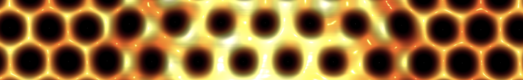
With that respect, two-dimensional Transition Metal dichalcogenides (TMDs), which are van der Waals supported layered structures, offer, by their very design, the promise of ultrathin high mobility channels with low leakage current that can help solving the problem of scaling. Unfortunately, current transistor and memory demonstrations made of synthetic materials remain disappointing, with electrical performances that differ strongly from their exfoliated material counterparts.
One of the main issues finds its origin in the current inability to grow a high-quality grain-less channel with deposition conditions compatible with current silicon CMOS standards, leading to defective, low mobility, high leakage polycrystalline materials. The resulting grain boundaries and vacancies, are not only the source of charge scattering, impacting the transport process, but also act as reactivity centres that may lead to oxidation and chemisorption reactions, hence degrading the device performances. Therefore, there is an urgent need to understand the mechanisms driving the TMD growth, and how the interplay between the substrate used for the material growth, the nature of the precursors, and the deposition conditions are impacting the growth mechanisms.
This post-doc position aims at solving this challenging issue by using the predictive power of first-principle simulations to model the different reaction mechanisms involved in the growth of transition metal dichalcogenides such as precursor diffusion and reactivity (activation energies), the impact of the substrate morphology on the nucleation (reactivity of surface step edges, defects,...) and the thermodynamic driving force for the formation of defects,... by combining state-of-the-art density functional calculations with thermodynamic and molecular dynamic simulations. The insights gained will provide precious information in terms of precursor selection and how deposition factors such as the precursor ratio, substrate treatments, temperature and pressure dependencies impact the material deposition process. The outcome of the simulations will be used systematically to drive experimental investigations.
more details
Please note that this project is in the framework of CSC-IMEC-KU Leuven Scholarships. Please read the requirements before applying here.