Job announcements relevant to people interested in electronic structure calculations…
The Psi-k forum mailing lists are now closed permanently. Please read this announcement about the new Psi-k mailing list.
PhD position: Controlling the position of dopant ... (No replies)
Back to Job listings...
For the last 60 years, randomly placed group III and V donors have been a key feature of semiconductor technology. The last decade has witnessed the development of deterministic doping, with the associated possibility of creating arbitrary low dimensional solids within the “vacuum” provided by the world’s cleanest host, silicon, as well as constructing new devices atom by atom. This capability is as significant for condensed matter and device physics as the development of cold atom technologies has been for atomic physics, and this PhD project forms part of a large programme (ADDRFSS) which aims to convert this view into reality. There will be a wide range of impacts, from the improvement of classical devices for which disorder-based scattering and localisation effects will be suppressed, through to integrated quantum gate networks.
Our experimental group have developed a strong UK capability for atomically precise dopant placement and device fabrication. The key stages of atomically-precise hydrogen resist patterning, phosphine deposition, encapsulation via silicon molecular beam epitaxy, and electrically contacting device layers have all been achieved, and are now routine in our laboratory. Our modelling approach, which complements and enhances experiment, is based on density functional theory (DFT), which is the most successful electronic structure technique in wide use. We use both standard DFT and linear scaling approaches, which allow us to model systems of exceptional size (100,000 to 1,000,000 atoms).
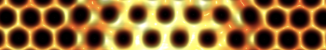
We are the first group to image and interpret the wavefunction of a substitutional dopant atom in silicon. The figure shows an STM image of a single arsenic atom located several atomic layers beneath a H-terminated Si(001) surface. This feature has a distinct anisotropic cross and line shape, covering multiple Si(001) dimer rows. We confirm that this feature is a neutral As donor, and identify the precise layer it is located in, by computing STM images using DFT and comparing to experiment.
The overall aim of the ADDRFSS project is to develop semiconductor engineering at the atomic scale to produce pairs, ordered 2-D arrays and ordered 3-D ‘lattices’ of single and multiple dopant atom species, embedded in Group IV semiconductors. We will learn how to place dopant atoms at determined positions in a silicon substrate, and how to incorporate new impurities such as other Group V donors, Group III acceptors and magnetic atoms. The PhD project will involve using DFT to model dopant incorporation and properties, working closely with the STM group.
This project is fully funded for four years, and is open to EU citizens. It is supervised by David Bowler, UCL. For enquiries, please contact [email protected] (@MillionAtomMan).